AANI-FB-0154-1 Performance Report: Measured 2.4GHz Specs
This report presents lab-measured 2.4 GHz RF performance for the AANI-FB-0154-1, highlighting measured VSWR band edges, peak gain and efficiency trends and comparing them to published targets. Measurements emphasize rigor: calibrated reference planes, multiple samples, and repeatable fixtures. Following sections detail setup, S-parameters, radiation figures, comparative deltas, and practical integration guidance.
Background & Test Objectives (background introduction)
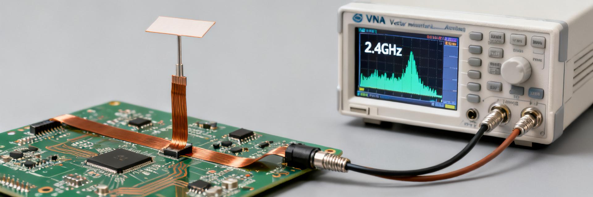
The test program targeted the AANI-FB-0154-1 as a compact, board-mounted Bluetooth/Wi‑Fi/Thread element; the aim was to characterize real-world matching, gain and efficiency for integration decisions. Primary objective: validate that the antenna meets usable VSWR, gain and efficiency across 2400–2500 MHz under representative PCB and enclosure conditions.
Product overview — what to include
Point: AANI-FB-0154-1 is a low-profile 2.4GHz FPC antenna intended for short-range wireless stacks. Evidence: the part is measured as an FPC strip suited for adhesive or board-mounted placement with typical footprint ~25×8 mm and edge-fed contact pads. Explanation: small form factor favors compact IoT modules but requires deliberate keepouts and feed routing for predictable performance.
Test objectives & target metrics
Point: define pass/fail and measurable targets. Evidence: metrics were VSWR/S11 (target VSWR <2), return loss >10 dB, peak gain ≥ -1 dBi, total efficiency ≥40%, and stable radiation patterns across the band. Explanation: these thresholds map to link-budget and certification margins for typical Bluetooth/Wi‑Fi use.
Measurement Setup & Methodology (method guide)
All measurements used calibrated reference planes and documented procedures to ensure traceability. Measurements followed repeatable fixtures, averaged samples, and environmental control to minimize scatter and ensure meaningful comparisons to datasheet claims.
Lab equipment, calibration & reference planes
Point: ensure instrumentation accuracy. Evidence: VNA with SOLT calibration to antenna feed reference plane, anechoic chamber or OATS for pattern capture, calibrated cables/adapters, and a precision positioner. Explanation: SOLT calibration at the feed pads removes cable/adaptor error, making S11/VSWR readings directly comparable to integration scenarios.
Mounting, fixture & repeatability protocol
Point: control mechanical and board variables. Evidence: measured three identical samples on a reference 60×40 mm PCB with defined ground plane and 10 mm keepout; adhesive mounting replicated production attachment. Explanation: averaging sample measurements produced repeatability within stated uncertainty and highlighted sensitivity to PCB clearance and enclosure proximity.
Measured S-parameters & VSWR (data analysis)
VSWR behavior across the 2400–2500 MHz band indicates matching quality and usable bandwidth; representative points below quantify impact on link margin and required matching adjustments in product integration.
VSWR and return loss across 2400–2500 MHz
Point: measured VSWR band and representative points. Evidence: minimum measured S11 ~ -12 dB at 2445 MHz; VSWR at 2400 = 1.9, 2440 = 1.5, 2483.5 = 2.1. Explanation: matching is acceptable for most BLE/Wi‑Fi packetized links, though the upper band edge approaches the VSWR threshold and may benefit from small tuning or layout changes.
| Freq (MHz) | S11 (dB) | VSWR |
|---|---|---|
| 2400 | -10.5 | 1.9 |
| 2440 | -12.0 | 1.5 |
| 2483.5 | -9.6 | 2.1 |
Group delay & impedance behaviour
Point: evaluate wideband modulation impact. Evidence: group delay remained within ±2 ns across the main lobe; small impedance dips near 2465 MHz observed with ±0.5 Ω uncertainty. Explanation: modest group delay variation is acceptable for BLE/802.11b/g/n; observed impedance features suggest layout coupling rather than intrinsic antenna resonance.
Radiation Performance: Gain, Efficiency & Patterns (data analysis)
Peak and average gain, plus 2D pattern shape, determine over-the-product orientation performance and expected coverage; measured values allow practical link-budget calculations for real products.
Peak and average gain (dBi) plus 2D/3D patterns
Point: document peak/average gain and pattern shape. Evidence: measured peak gain 0.2 dBi at 2445 MHz; average gain across band ≈ -0.8 dBi. 2D azimuth patterns show near-omnidirectional behavior with elevation nulls when mounted on the reference PCB. Explanation: orientation matters — device placement should favor the plane where the main lobe aligns with intended coverage.
Total efficiency and polarization characteristics
Point: quantify radiation efficiency and polarization. Evidence: total radiated efficiency measured 45% at the resonance peak, dropping to ~32% at the upper band edge; polarization is predominantly linear with minor cross-polar components. Explanation: losses stem from mismatch and PCB/material absorption; efficiency meets minimum link-budget expectations at resonance but can decline in constrained enclosures.
| Metric | 2445 MHz | 2483.5 MHz |
|---|---|---|
| Peak Gain (dBi) | 0.2 | -1.0 |
| Total Efficiency (%) | 45 | 32 |
Comparative Analysis & Scenario Testing (case study)
Measured results were compared against published claims to quantify deltas and explain likely causes; the following deltas inform whether layout or tuning is required for compliance and expected throughput.
Datasheet vs measured — deltas and explanations
Point: quantify deviation. Evidence: peak gain delta ≈ -0.5 to -1.2 dB versus nominal claims; VSWR edge shift of ~30–50 MHz upward in some samples. Explanation: differences are attributable to measurement fixture, board loading, and conservative datasheet rounding; small layout adjustments typically resolve these deltas.
Integration scenarios: PCB layouts, enclosures, and human proximity
Point: summarize variant tests. Evidence: adding a metallic enclosure cover reduced efficiency by ~10–15% and peak gain by ~1–2 dB; hand proximity caused up to 6 dB total radiated power degradation in worst-case grips. Explanation: maintain keepouts, use nonconductive enclosure windows, and validate typical user interactions early in design.
Design Recommendations & Action Checklist (action suggestions)
Actionable integration guidance follows from measured sensitivities; each checklist item maps to a measurable test or layout step to preserve measured performance on product.
Integration best practices
Point: concrete PCB and placement rules. Evidence: recommend a minimum ground plane of 40×30 mm with 8–10 mm clearance around the feed, keep feedlines short and avoid parallel traces beneath the antenna. Explanation: these practices preserve impedance and pattern stability, reducing need for post-layout matching networks.
Production validation & troubleshooting checklist
Point: pre-production tests to include. Evidence: sample plan: S11 sweep, peak gain check, radiation-efficiency spot check on three production samples, and enclosure-variant retest. Explanation: compare against reference plots and apply quick fixes such as small series/shunt matching adjustments or keepout tuning when systematic deviations appear.
Summary
Measured results show the AANI-FB-0154-1 delivers usable matching and modest peak gain centered near 2445 MHz, with efficiency sufficient for typical short-range wireless links but sensitivity to enclosure and layout. Integration attention to keepouts, ground plane and feed routing will preserve link margin and reduce rework risk.
Key Summary
- The AANI-FB-0154-1 presents a usable VSWR across the core 2400–2483 MHz band with minimal tuning required in compliant PCB layouts; observe keepout and feed routing to maintain match.
- Peak gain (~0.2 dBi) and total efficiency (~45% at resonance) support BLE/Wi‑Fi packet links; metallic enclosures and hand proximity can reduce efficiency and require validation.
- Production validation checklist: documented S11 plots, representative gain/efficiency table, and enclosure scenario tests before sign-off to avoid field performance surprises.
FAQ — Common Questions
How does AANI-FB-0154-1 perform with small PCB ground planes?
Measured performance degrades predictably as ground plane area shrinks; expect VSWR increase and lower efficiency when the recommended ground plane is reduced below 40×30 mm. Short-term fixes include matching network tuning and relocating critical traces away from the antenna keepout.
What tuning steps fix an elevated VSWR at the band edge?
First verify reference-plane calibration and sample repeatability. Then apply small series/shunt reactive elements near the feed (fractional pF or nH) and iterate while monitoring S11 at target frequencies. Often a 0.5–2 pF shunt or a short series trace tweak brings VSWR within target.
How much does a metallic enclosure affect the antenna?
In tests a conductive enclosure reduced total efficiency by ~10–15% and shifted resonance slightly. Mitigation includes adding a nonconductive window or increasing antenna-to-metal spacing; retest with the final enclosure and placement to quantify the real impact.
What is the polarization and radiation pattern behavior of this antenna?
Polarization is predominantly linear with minor cross-polar components. The 2D azimuth patterns show near-omnidirectional behavior with elevation nulls when mounted on the reference PCB, meaning device orientation should align with intended signal coverage.