


Helping you save cost and time.

Provide reliable packaging for your goods.

Quick and reliable delivery to save time.

Excellent after-sales service.
New Product Launch
More +

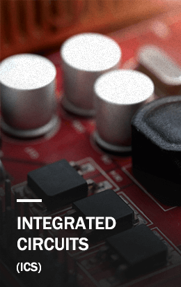
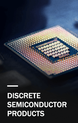
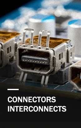
Hot Selling Parts


Blog

AANI-FB-0174-1 FPC Antenna: Performance Report & Stats
The AANI-FB-0174-1 demonstrates a practical cellular/IoT fit with an effective measured frequency span of 1.71–2.69 GHz, a typical peak gain near 2.7 dBi, and reported radiation efficiency around 59% …
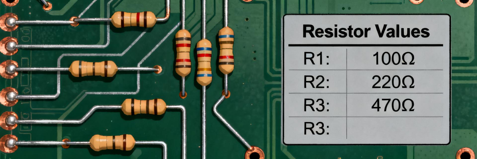
Resistor Market Pulse: Key Metrics & Component Usage
A strategic analysis of global trends, demand catalysts, and procurement benchmarks. The current snapshot shows the resistor market positioned between a steady-demand cycle and pockets of rapid volume…
0603 20kOhm 1% resistor: Supply, Specs & Pricing Guide
2026-04-30 10:17:17
RC0402FR-070RL Specs & How to Use 0402 Jumper Safely
2026-04-29 10:17:19
RC0402JR-071ML datasheet: 1MΩ 0402 SMD specs & test data
2026-04-26 10:26:14
0402 Zero-Ohm Resistor Market & Spec Snapshot — Latest Trends
2026-04-24 10:19:21
RC0402JR-07100KL Datasheet: Measured Specs & Yield
2026-04-15 10:18:18
Read more